Conductive vs. Non Conductive Via Filling: Choosing the Right Approach for Your PCBAuthor : Adrian September 03,pewter solder paste 2025Table of ContentsWhen designing a printed circuit board (PCB), one critical decision is whether to use conductive or non-conductive via filling. This choice impacts your board’s performance, reliability, and cost. In short, conductive via filling excels in enhancing electrical and thermal conductivity, while non-conductive via filling is ideal for structural support and cost-effective applications. In this blog, we’ll dive deep into the benefits, applications, and key considerations like thermal conductivity, electrical conductivity, and CTE mismatch in via filling to help you make the best decision for your project.
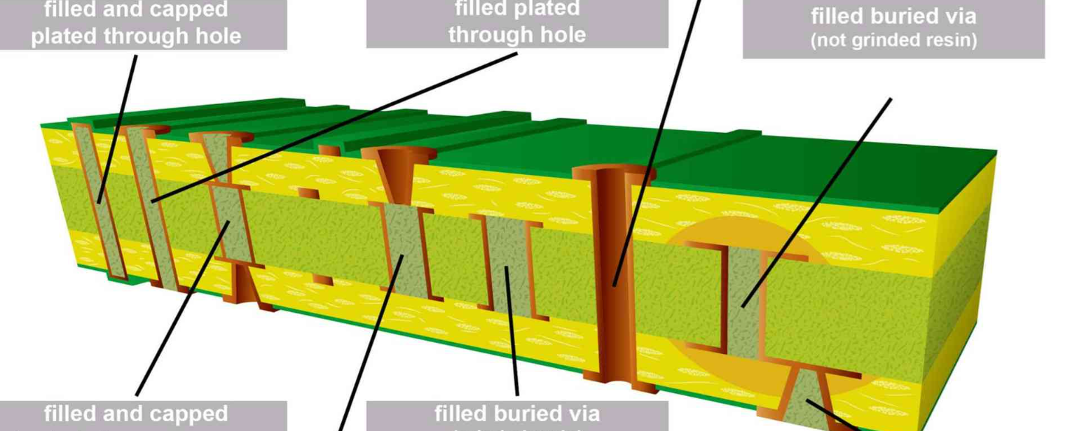
Understanding Vias and Via Filling in PCB DesignVias are small holes in a PCB that connect different layers of the board, allowing electrical signals or power to pass through. However, unfilled vias can lead to issues like air entrapment, weak structural integrity, or poor thermal management. Via filling solves these problems by filling the holes with either conductive or non-conductive materials, depending on the design needs. Via filling is especially critical in high-density interconnect (HDI) boards, where space is tight, and performance demands are high. The choice between conductive and non-conductive filling depends on factors like electrical requirements, thermal dissipation needs, and budget constraints. Let’s explore both options in detail to understand their unique advantages and use cases.
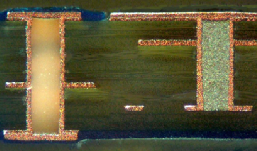
What Is Conductive Via Filling?Conductive via filling involves filling the via holes with a material that conducts electricity, such as copper or silver epoxy. This method ensures a continuous electrical path through the via, making it an active part of the circuit. Conductive fills are often used in applications where signal integrity and thermal management are top priorities. Conductive Via Filling BenefitsChoosing conductive via filling offers several advantages, especially for high-performance designs. Here are the key benefits:
These benefits make conductive via filling a go-to choice for advanced PCB designs, especially in industries like telecommunications, aerospace, and automotive electronics.
What Is Non-Conductive Via Filling?Non-conductive via filling uses materials like epoxy resin that do not conduct electricity. This method focuses on providing structural support and protecting the via from environmental factors rather than contributing to the circuit’s electrical performance. Non-conductive fills are often more cost-effective and easier to apply compared to conductive options. Non-Conductive Via Filling ApplicationsNon-conductive via filling is widely used in scenarios where electrical conductivity through the via is not required. Here are some common applications:
Non-conductive via filling shines in applications where the primary goal is durability and cost savings rather than electrical or thermal performance.
Comparing Thermal Conductivity of Filled ViasThermal management is a critical factor in PCB design, especially for devices that generate significant heat, like power supplies or LED lighting systems. The thermal conductivity of filled vias plays a big role in how effectively heat is dissipated across the board. Conductive via fills, particularly those using copper, offer superior thermal conductivity. Copper has a thermal conductivity of approximately 385 W/m·K, allowing it to transfer heat quickly from hot spots to heat sinks or other cooling mechanisms. This makes conductive fills ideal for high-power applications where thermal buildup can damage components or reduce performance. On the other hand, non-conductive via fills, such as epoxy, have much lower thermal conductivity, often below 0.5 W/m·K. While they provide some insulation, they are not effective at dissipating heat. In designs where heat management is a concern, relying solely on non-conductive fills might require additional cooling solutions, increasing overall costs. For example, in a high-power LED board, using conductive via filling can reduce junction temperatures by up to 10-15°C compared to non-conductive fills, significantly improving reliability. If thermal dissipation is a priority, conductive filling is often the better choice.
Evaluating Electrical Conductivity of Filled ViasElectrical conductivity is another crucial aspect when choosing between conductive and non-conductive via filling. Conductive fills are designed to carry current, making them essential for maintaining signal integrity and power distribution in a PCB. Copper-filled vias, for instance, provide excellent electrical conductivity with minimal resistance. This ensures that signals traveling through the via experience low loss, which is vital for high-speed circuits operating at frequencies above 500 MHz. In contrast, non-conductive fills act as insulators, blocking electrical flow through the via. While this is useful for isolating certain layers, it means the via cannot be part of the active circuit. In practical terms, if you’re designing a board for a high-speed processor, conductive via filling can help maintain signal integrity by keeping impedance consistent across layers. Non-conductive fills, however, might be more suitable for simpler designs where vias only serve a mechanical purpose, and electrical paths are managed elsewhere on the board.
Addressing CTE Mismatch in Via FillingCoefficient of Thermal Expansion (CTE) mismatch is a significant concern in via filling, as it can lead to mechanical stress and reliability issues. CTE refers to how much a material expands or contracts with temperature changes. A mismatch between the CTE of the via fill material and the surrounding PCB materials (like copper or FR-4 substrate) can cause cracks, delamination, or via failure over time. Conductive via fills, such as copper, have a CTE of about 17 ppm/°C, which closely matches the CTE of the copper traces on the PCB (also around 17 ppm/°C). This compatibility reduces stress during thermal cycling, making conductive fills a reliable choice for applications with frequent temperature fluctuations, such as automotive electronics. Non-conductive epoxy fills, however, often have a higher CTE, ranging from 30 to 60 ppm/°C, compared to the PCB substrate (typically 14-18 ppm/°C for FR-4). This mismatch can lead to stress buildup, especially in boards exposed to extreme temperatures. To mitigate this, designers may need to use specialized low-CTE epoxies or limit the use of non-conductive fills in thermally demanding environments. For instance, in a PCB designed for aerospace applications with temperature swings from -40°C to 85°C, a conductive fill might prevent via cracking better than a standard epoxy fill due to better CTE alignment. Careful material selection and design considerations are key to managing CTE mismatch in via filling.
Key Factors to Consider When Choosing Via FillingDeciding between conductive and non-conductive via filling requires balancing several factors based on your project’s needs. Here are the main considerations:
By weighing these factors, you can select the via filling method that aligns with your design goals and constraints.
Practical Tips for Implementing Via Filling in Your DesignTo ensure the best results with via filling, keep these practical tips in mind during the design and manufacturing stages:
Following these guidelines can help you achieve a robust and reliable PCB design tailored to your specific needs.
Conclusion: Making the Right Choice for Your PCBChoosing between conductive and non-conductive via filling is a pivotal decision in PCB design that affects performance, reliability, and cost. Conductive via filling offers unmatched benefits in electrical conductivity and thermal dissipation, making it ideal for high-performance applications like high-speed circuits and power electronics. Non-conductive via filling, on the other hand, provides cost-effective structural support and protection, fitting well in simpler or budget-conscious designs. Consider factors like thermal conductivity of filled vias, electrical conductivity requirements, and CTE mismatch in via filling to guide your decision. By understanding the unique strengths of each approach and aligning them with your project’s demands, you can create a PCB that meets both technical and economic goals. Whether you prioritize signal integrity or structural durability, the right via filling method will elevate your design to the next level. Share · · · · The Role of Flux in PCB Wave Soldering: Selection, Application, and Residue RemovalMarch 16, 2026PCB wave soldering flux types include rosin, water-soluble, and no-clean options with varying activity levels for oxide removal and solder flow. This guide covers selection criteria, spray foam drop-jet application methods, residue removal processes, and alternatives like nitrogen blanketing to boost joint reliability and yields for engineers. Article Achieving Uniform Solder Fillets in PCB Wave Soldering: Process ControlMarch 16, 2026Achieve uniform solder fillets in PCB wave soldering with process control strategies. Optimize flux, preheat, wave height, conveyor speed for consistent fillet shape, height, and wetting balance. Includes visual inspection tips and troubleshooting for reliable through-hole assemblies. Boost quality in production. Article Optimizing Conveyor Speed for Efficient PCB Wave SolderingMarch 16, 2026Learn PCB wave soldering conveyor speed calculation to manage dwell time, immersion depth, and throughput effectively. Electric engineers get practical steps, best practices, and troubleshooting tips for higher process efficiency and fewer defects in wave soldering operations. Article Understanding IPC Standards for PCB Surface Finishes: Ensuring Quality and ComplianceMarch 11, 2026Understand IPC standards IPC 4552 ENIG and IPC 4553 immersion silver for PCB surface finishes. Ensure compliance, enhance solderability, and prevent common defects to achieve reliable, high quality circuit boards. Article Miniaturization Challenges in PCB AssemblyMarch 11, 2026Navigate the complexities of high density interconnect PCB assembly and precise component placement. Learn to tackle miniaturization challenges, from tiny part handling to thermal stress, ensuring robust and reliable electronics. Article High Speed Routing Techniques: PCBMarch 11, 2026Master high speed routing in PCBs to ensure signal integrity and minimize electromagnetic interference. Learn essential techniques for robust designs, from controlled impedance to differential pair strategies. Prevent performance issues and achieve reliable electronics. ArticleGet Instant PCB |